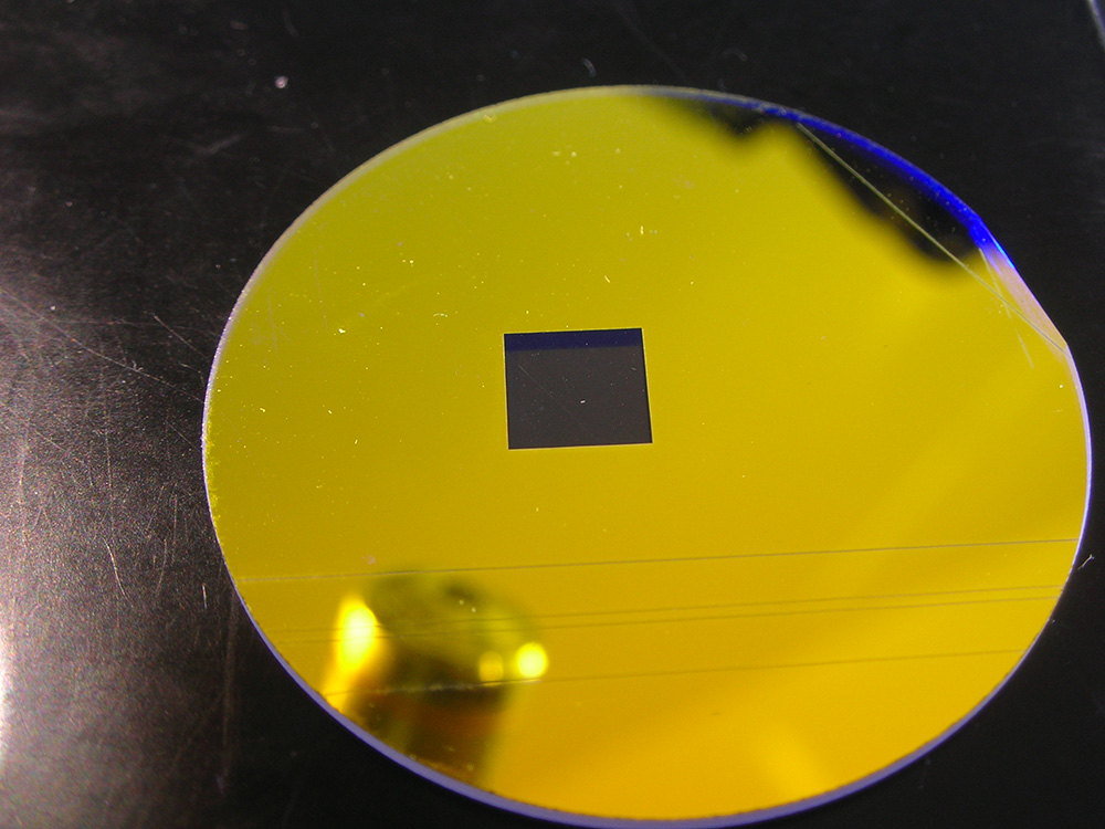
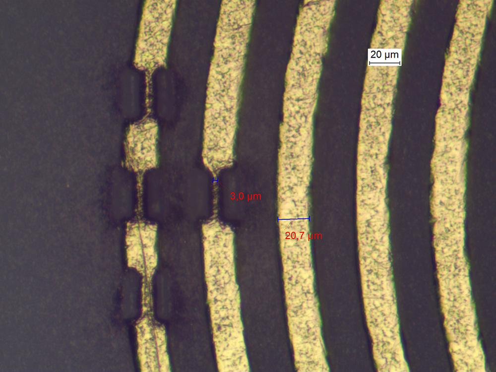
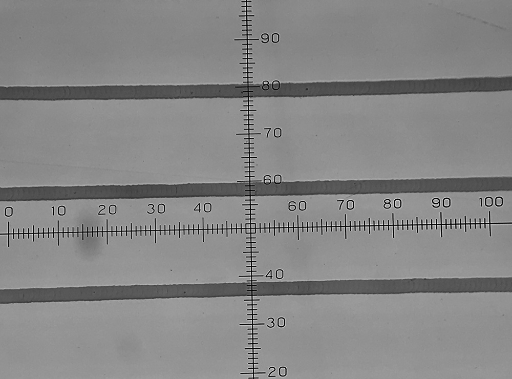
This laser process is characterized by a very clean and controlled ablation of thin layers by keeping the substrate undamaged. The minimum ablated feature is in the range of a few micrometers and correction of RF circuits and components, displays and many others thin film devices.